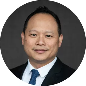
Mr. Lee Peng CHUA
Director of Technology of Sabre 3D platform, Lam Research
Lee Peng CHUA is a Director of Technology of Sabre 3D platform in the WETS Metals business unit at Lam research. He has been at Lam Research for 22 years, and is now responsible for technology and process development pertaining to TSV (through silicon via) and WLP (wafer level packaging) electrodeposition. Prior to that, he had worked on process and technology development in High Density Plasma HDP and Plasma Enhanced Chemical Vapor Deposition (PECVD). Lee earned his Master’s in Chemical Engineering at Purdue University, and has over 20 patents.
Presentation Title
Enabling heterogenous integration interconnects with equipment technology solutions
Abstract
The semiconductor industry continues to evolve at a rapid pace by the demands of diverse applications spanning from artificial intelligence (AI) and 5G communication to automotive and IoT, whereby advanced semiconductor packaging is ever becoming more integral in meeting high performance requirements at a cost effective solution. Various levels and architecture complexities emerges, deployed by application, such as: fan-out wafer-level packaging (FOWLP), heterogeneous integration System in package (SIP) and chiplets, and 3D integrated circuits (3DIC). These advancing package architectures drive the need for interconnect density increase, miniaturization, and material innovation. To meet these demands, Lam Research is constantly pushing the boundaries of technology in the fabrication of these interconnect building blocks: microbump, fine line redistribution layer (RDL), megapillar, through silicon via (TSV), and newer hybrid bonding technology. We will delve into key trends, requirements, challenges and Lam Research innovative solutions in this space.
Back to Chiplet Technology & Heterogeneous Integration Summit