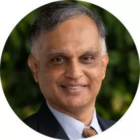
Dr. Surya BHATTACHARYA
SEMI Southeast Asia Advanced Product Testing Technical Committee | Director, Head System in Package, Institute of Microelectronics (IME), A*STAR
Dr. Surya Bhattacharya (Senior Member IEEE) is Director and Head of System-in-Package at A*STAR Institute of Microelectronics (IME), Singapore. Over the past 30 years, he has worked on CMOS scaling and Package Scaling at fabless companies, integrated device manufacturer (IDM), and leading Research Institute. At the Institute of Microelectronics, Singapore, Dr. Bhattacharya leads the advanced packaging team to initiate and execute consortia projects to address industry challenges in advanced heterogeneous integration for system scaling. Prior to joining IME, he served as Director of Foundry Engineering at Qualcomm, where he executed technology and manufacturing ramps across multiple foundries around the world. Prior to Qualcomm, he was a Principal Foundry Engineer at Broadcom Corporation. He started his career at Rockwell Semiconductor Systems, Newport Beach, California, where he was Senior Manager for CMOS technology development. Surya has a PhD in Electrical Engineering from the University of Texas at Austin, and B.Tech in Electrical Engineering from the Indian Institute of Technology, Madras.
Presentation Title
Advanced Multi-Chiplet Heterogeneous Integration Packaging for AI and High-Performance Computing
Abstract
AI and High-Performance Computing (HPC) are key driving forces for in-package scaling for advanced computer systems. Advanced System-in-package (SiP) scaling enables the long-term roadmap for continued power, performance, form-factor and cost optimization of HPC-systems. Advanced SiP typically integrates multiple heterogeneous chiplets namely, xPU, Memory, and I/O chiplets, and hundreds of thousands of such SiPs are interconnected in servers and racks across a hyper-scale data centre to reach exaflops to zettaflops of compute performance targets to meet the growing needs of generative AI over the coming decade. Interconnecting chiplets within a SiP and interconnecting SiPs in an energy-efficient manner demands fabrication of high-density/high-speed/high-bandwidth 2D, 2.5D and 3D electrical and optical interconnects for the SiP. The SiP needs to have the ability to handle electrical-to-optical (E-O) and O-E conversion at pj/bit energy efficiencies and Tbps/mm bandwidth densities in addition to providing mechanical stability and thermal cooling for power hungry (>200W/cm2) xPU chiplets. Multi-chiplet heterogeneous integration (MCHI) is the critical technology that enables the realization of such complex energy-efficient advanced SiP which forms the basic building block for HPC systems of today and future. In this presentation, we will discuss the key technologies developed by IME-Singapore to enable the industry to perform pathfinding, design, fabrication, assembly and prototyping of MCHI SiP for AI and HPC. We will also present how IME drives collaborative R&D across the entire semiconductor ecosystem to accelerate the development and translation of advanced multi-chiplet packaging.
Back to Advanced Packaging & Heterogeneous Integration Summit