
Advanced Packaging & Heterogeneous Integration Summit | Day 2 | 21 May 2025, Wednesday | 10:00 - 17:30hrs | L3 | Heliconia | 3410A - 3511
Explore the cutting-edge advancements transforming the semiconductor industry at the Advanced Packaging and Heterogeneous Integration Summit. This event focuses on innovative packaging solutions for chiplet integration and the expanding opportunities in silicon photonics.
Bringing together speakers from across the value chain—materials, equipment, design, packaging, and end-users—it offers a holistic view of the innovations driving performance, power efficiency, and scalability. Key topics include advanced packaging architectures, heterogeneous integration strategies, advanced packaging techniques like fan-out panel-level packaging (FOPLP) and Co-Packaged Optics (CPO) in emerging application such as silicon photonics for data centers and telecommunications.
Engage in thought-provoking discussions, gain valuable insights into industry challenges and solutions, and connect with key players shaping the future of semiconductor technologies. Join us at the summit to discover how advanced packaging and heterogeneous integration are unlocking the potential of tomorrow’s innovations.
Registration is open!
EARLY BIRD RATE | PUBLISHED RATE | STUDENT | ||
SEMI-Member | Non-Member | SEMI-Member | Non-Member | |
350 | 450 | 440 | 570 | 75 |
- All prices listed are in Singapore Dollars and subject to 9% GST, applicable only to Singapore-based companies for pre-registration.
- For on-site registration (subject to seats availability), a 9% GST will be applied, regardless of the company's location.
- Group purchases of 3 or more participants (in a single registration) will receive a 15% discount.
- Ticket purchased are strictly non-refundable and non-transferable.
- For HRD Corp claims (only for Malaysia attendees), please refer to the following links on the claiming matrix and guidelines:
Agenda
Session Chairs:

Mr. Samuel GOH
Senior Director, AP Product Marketing, Kulicke & Soffa |
Chairman, SEMI Southeast Asia Advanced Packaging Technical Committee, Singapore

Dr. Suresh Kumar SINGARAM
Head of Asian Technical Task Force, Evatec AG |
Vice Chairman, SEMI Southeast Asia Advanced Packaging Technical Committee, Singapore
| Time | Program |
|---|---|
| 10:00 - 10:05 hrs | Welcome and Introduction |
10:05 - 10:30 hrs | Keynote: Emergence of Chiplet and New Era of Advanced Packaging Dr. BJ HAN, Chief Executive Officer & Co-Founder, Silicon Box, Singapore |
| 10:30 - 10:55 hrs | Keynote: Propelling AI forward through Advanced Packaging Creativity Mr. Ingu Yin CHANG, Executive Vice President, ASE, United States |
| 10:55 - 11:15 hrs | From Complexity to Capability: Enabling Breakthroughs in Critical Advanced Packaging Technologies Mr. Terrance LEE, Vice President, Heterogenous Integration Business Unit, Semiconductor Products Group, Applied Materials, United States |
| 11:15 - 11:30 hrs | Break & Networking |
| 11:30 - 11:50 hrs | Advanced Packaging Market, Technology, and Manufacturing Trends Mr. John WEST, Chief Analyst, Semiconductor Equipment, Yole Group, France |
| 11:50 - 12:10 hrs | Advanced Multi-Chiplet Heterogeneous Integration Packaging for AI and High Performance Computing Dr. Surya BHATTACHARYA, Director, Head System in Package, Institute of Microelectronics (IME), A*STAR | SEMI Southeast Asia Advanced Packaging Technical Committee, Singapore |
| 12:10 - 12:30 hrs | Panel Level Packaging: Challenges and Advantages in Packaging R&D and High-Volume Production Mr. David GANI, Director, Back-end Manufacturing and Technology R&D, STMicroelectronics, Singapore |
| 12:30 - 12:35 hrs | Presentation of Token of Appreciation |
| 12:35 - 13:35 hrs | Lunch & Networking |
| 13:35 - 13:55 hrs | Packaging the Future: How Equipment Advancements are Enabling Heterogeneous Integration Mr. Chee Ping LEE, Managing Director, Strategic & Technical Marketing, Lam Research, Singapore |
| 13:55 - 14:15 hrs | WBG Technology Shaping Future Packaging Innovation Mr. Jan Sing LOH, Vice President, Backend Development Singapore | Chief R&D Officer, Indonesia, Infineon Technologies Asia Pacific, Singapore |
| 14:15 - 14:35 hrs | Pioneering Advanced Packaging Solutions for Heterogeneous Integration in Chiplet Ecosystems and Silicon Photonics Dr. Gary WIDDOWSON, Senior Vice President and Chief Technology Officer, ASMPT Semiconductor Solutions, Singapore |
| 14:35 - 14:55 hrs | Addressing Fine Pitch Bonding Challenges via Fluxless TCB Mr. Samuel GOH, Senior Director, AP Product Marketing, Kulicke & Soffa | Chairman, SEMI Southeast Asia Advanced Packaging Technical Committee, Singapore |
| 14:55 - 15:15 hrs | Advancements in Panel Level Sputtering Mr. Markus Christian FREI, Senior Product Marketing Manager, Advanced Packaging and Semiconductor, Evatec AG, Switzerland |
| 15:15 - 15:30 hrs | Break & Networking |
| 15:30 - 15:50 hrs | 3rd Generation Panel Level FOPLP for Integrated Optical Module and High Power Package Mr. Steve JIN, Chief Executive Officer, OIP Technology, Singapore |
| 15:50 - 16:10 hrs | Process, Hardware and Integration: Synergy for Advanced Packaging Tools Dr. James PAPANU, Senior Director, 3DI Technology, Tokyo Electron, Japan |
| 16:10 - 16:30 hrs | Advanced Packaging Materials Innovation through Co-Creative Activities Mr. Hidenori ABE, CTO for Semiconductor Materials, Resonac Holdings Corporation | Executive Director, Electronics Business Headquarters, Resonac Corporation, Japan |
| 16:30 - 16:50 hrs | Advanced Packaging Material Innovations Addressing Mechanical, Thermal, and Reliability Challenges in High-Performance Computing Applications Dr. Rose GUINO, Head of Application Engineering, SEA, Electronics, Henkel, Singapore |
| 16:50 - 17:10 hrs | Evolution of Inspection and Metrology in the AI Era Mr. Eyal SEGEV, Marketing Director, Semiconductor Equipment, Camtek, Israel |
| 17:10 - 17:30 hrs | Presentation of Token of Appreciation & Closing Remarks |
*Program subject to changes
Featured Speakers
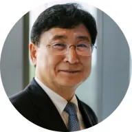
Dr. BJ HAN - Keynote Speaker

Mr. Ingu Yin CHANG - Keynote Speaker
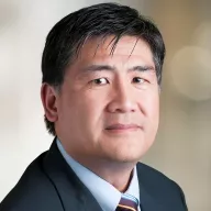
Mr. Terrance LEE

Dr. Gary WIDDOWSON
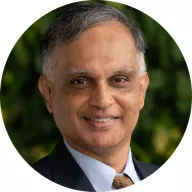
Dr. Surya BHATTACHARYA
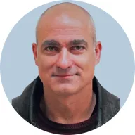
Mr. Eyal SEGEV

Mr. Markus Christian FREI

Dr. Rose GUINO
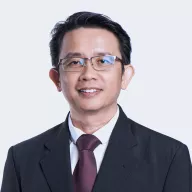
Mr. Jan Sing LOH

Mr. Samuel GOH
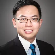
Mr. Chee Ping LEE
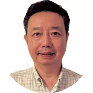
Mr. Steve JIN
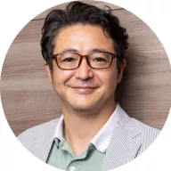
Mr. Hidenori ABE
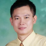
Mr. David GANI

Dr. James PAPANU